PCB Fabrication Enhancements
Extraction of Array Nesting
aPriori 2024 R1 SP3 extends the geometry extraction for the PCB Fabrication process group to capture the array nesting layout from Gerber and ODB++ files, allowing the user to view the proposed nesting from the ECAD design.
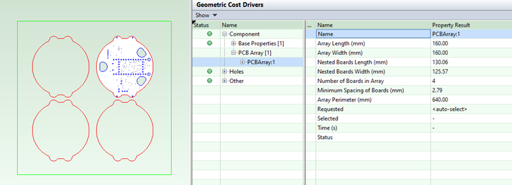
aPriori 2024 R1 SP3 extends geometry extraction to capture the array nesting layout for the PCB, if this layout is included in the model. When selected, a new GCD type, PCB Array, displays the nested outline in the viewer. The PCB Array GCD properties capture:
-
Array width and length
-
Nested boards length and width (bounding box of boards)
-
Number of boards in array
-
Minimum board spacing
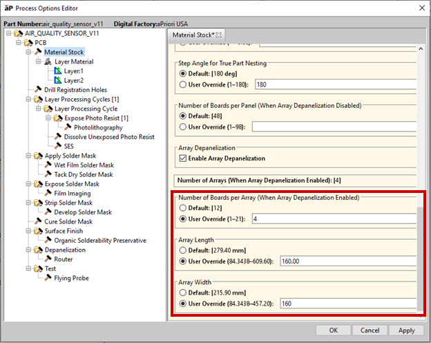
In aPriori 2024 R1 SP3, the GCD is for informational purposes only and can be used to visually verify that the aPriori nesting diagram matches the designed nesting. If the aPriori computed nesting does not match the extracted nesting, you can use material process setup options to correct the utilization—see example below.
In a future release, the PCB manufacturing process model will use the PCB Array GCD to compute material utilization for the designed nesting automatically.
For example:
PCB Array GCD read from ECAD file:
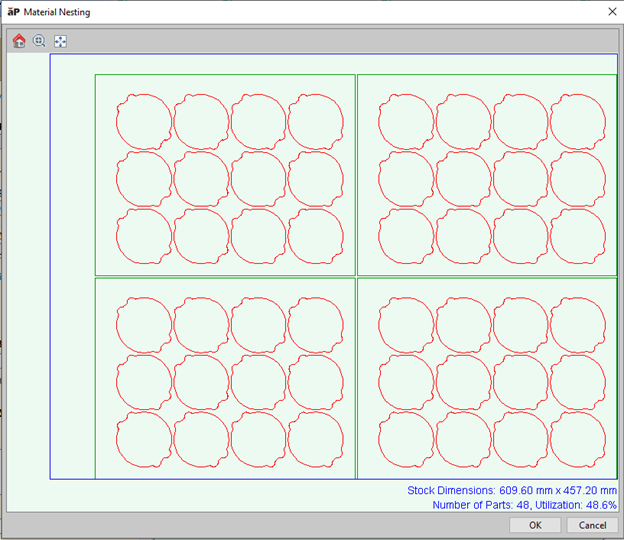
The aPriori out-of-the-box nesting is significantly different:
You can manually update the array process setup options to match the extracted GCD properties and calculate a material utilization estimate in line with the deigned array layout: