PCB Costing Workflow
PCB Cost Process Overview
To cost a PCB, aPriori:
-
Extracts all the GCD information from a source file containing all the GCD information for that PCB.
Note:
For the PCB Process Group, GCDs are extracted from either Gerber or ODB++ ECAD design files, rather than a 3D CAD Model.
-
Names and categorizes these GCDs, as for other groups in aPriori.
- Calculates a cost estimate for the PCB, considering aspects such as: Cycle Time, Labor Costs, Tooling Costs, Machine Overhead cost and Raw Material Cost.
See Cost a PCB for more details of the process.
Geometry Extraction Details
The following Information is extracted from the ODB++, Gerber, and drill files as GCDs:
- Component: represents the board as a whole. Properties include Length, Width, and Perimeter. In addition, information about the shape of the board outline is extracted and can be used in the calculation of material utilization.
- Layer: represents a copper layer. Note that each copper layer may be part of a 1-ply or 2-ply core, or it may be a standalone copper sheet.
- Common Holes: represents a group of holes that all share the same diameter, start layer, and end layer.
- Contour: represents a slot in the board used, for example, to align electrical components of the printed circuit board assembly.
PCB Layers
A completed production line PCB contains a number of conductive and insulative layers, as defined by the product specification. For example:
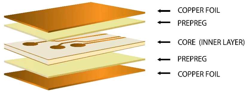
Note:
By default, aPriori supports up to 12 layers - this can be extended if needed.
aPriori supports both Rigid Single Layer Single-Sided and Rigid Multi-Layer Double Sided variants; for the Multi-Layer variant these layers must be stacked in an even format.
Layers and Vias
In correlation to the layers, it is also important to recognise that vias will significantly impact manufacturing.
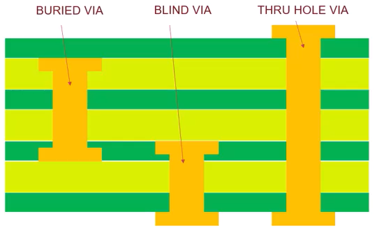
- A buried via is designed to connect inner layers and are not visible on any outer layers.
- A blind via is designed to connect from either one of the outer layers to an inner layer but does not extend through the board to the next outer layer.
- A through hole via can pass from one outer layer through the internal layers out to the second outer layer.
Example.
This example illustrates the common types of layers found on a PCB board.
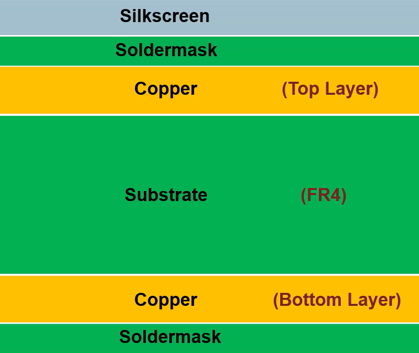
Working out from the center:
-
The central substrate layer between the two copper areas provides rigidity and structure to the board. This layer is typically made using FR4 fibreglass material.
-
The copper top and bottom layers are required to link all the components within the circuitry together. These layers are made from copper based primarily upon its conductive properties.
-
The outer soldermask layers protect the copper tracks from oxidation (which would lead to corrosion in the field) and helps prevent unintentional solder connections when components are connected to the board. This layer is typically made using polymers of different grades resembling a lacquer consistency.
-
The top silkscreen layer includes traces of non-conductive epoxy (an ink-like substance) mapping out where to locate the given components on the board or provide additional text information, such as polarity, test point indication, or product identification codes.
Differing PCB material type and offerings can be supported with each of these materials having an associated gauge.
Panels
PCBs are generally produced in volume, usually in panel format, with each panel containing multiple PCBs.
aPriori supports multiple ranges of panel size dimensions by default, and you can adjust nesting patterns based on your requirements.
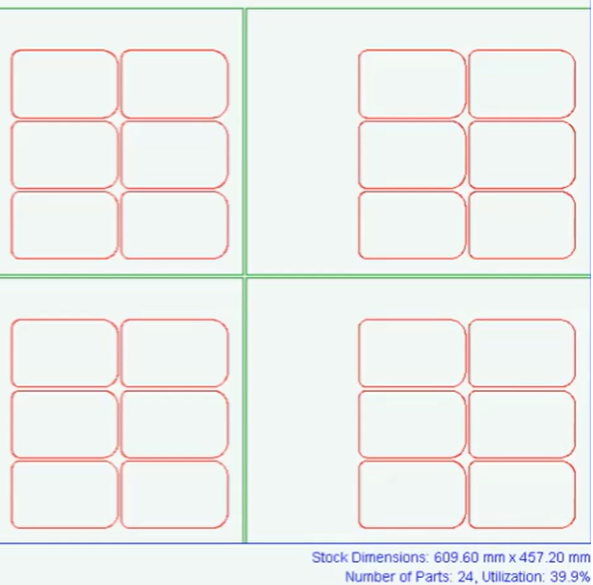
You can enable or disable array panelization; this is a PCB technique that helps to reduce cost and allows for efficiency in assembly, placing multiple copies of the board in an array on a panel format. On completion they can then go through depanelization where they are broken away from the panel readily using tabs.